Toner Transfer method for making PCB at home is probably one thing that went as viral as the Arduino. Electronics hobbyists around the world started using it to make professional looking PCBs at home. Here I will document the steps involved in fabricating PCBs with things that you can mostly find off the shelf.

Before getting to the details in the making your own PCBs I wish to share an old experience. So, if you have left the soldering iron turned on you can skip it and jump straight into the content.
The first time I saw a PCB made at home was around 2005. My brother, an electronics enthusiast and hobbyist made an audio amplifier for a broken music system. Back then, I din’t know if this method was yet to be introduced or we overlooked it, we were in stone age.
We did not have any means to transfer the layout to the copper clad board as such. So we took a print out of the silk screen layer and pasted it over the non copper side of the board. Then we drilled all the holes into the clad board. Once this was done, we took a printout of the bottom layer and started connecting the dots with a marker pen according to the layout image.
Once all the dots were connected, we started to thicken the lines and also covered the pads. All this was done manually and we proceeded to the etching process. The endeavor took us a whole day and I’m happy to inform that the board still works (to-date) like a charm.
Toner Transfer Method -An Underlying Theory
Originally this method was to be used with photo paper. They did not become very popular due to two reasons. First the paper is very costly (compared to the kind of paper used for this tutorial). Next the plastic coat that they have over them seemed to bond very tightly with the copper and hence making it difficult to remove the paper after the toner has fully been transferred to the clad board.
The toner or the ink from the laser printer is a kind of plastic. When heated, this ink melts and and loses its affinity to the paper. At such a time, with proper pressure and optimum heat, the copper clad board posses a higher attraction to the molten ink. That is when the toner is transferred to the copper surface.
Even after the ink is transferred to the copper surface the ink is not yet fully attached to it. A very basic lesson in physics tells us that copper can retain heat for a relatively longer period of time. So you will have to allow it to cool and let the ink establish its grip over the surface.
Once the ink is on the copper it forms a protective coating and keeps away the etchant from touching the copper under it’s control. This way the tracks are preserved when they are subjected to the corrosive effect of the ferric chloride solution.
This method is really easy to follow and you can jump into action by just seeing the images that I have posted below (which you are free to do) but you’ll soon realize that there is one hell lot of things to learn from making mistakes. So it’s advisable to go through the few words I have added to each of the steps below.
Here is a tip, don’t try to learn from your own mistakes while making PCBs. One small mistake will force to go back to step one which is a laborious and a daunting task.
Print the design on the Toner Transfer Paper
Recently, I purchased PCB papers from eBay and wanted to see the results of the new investments and quite frankly, I’m impressed. I downloaded an open source Pickit2 design and made some alterations to suit my needs and got it printed on the paper.

I could print, as you can see 8 images in one sheet after a lot of modification to the design and its orientation.
Prepare the copper clad board
The next step is to prepare the copper clad board for the toner transfer. The toner sticks on to copper that is free from oxidation and any oil stains. Even the moisture in your hands could spoil the transfer. So use proper detergent to clean the copper board. Spend enough time in this process as the steps that follow rely on how well you did this.

Don’t touch it!
Once you feel that the copper is really clean and doesn’t need any more scrubbing, rinse it in water. DO NOT use your hands to wipe away the detergent or the water. Just hold it in running water for some time and then let it dry in an inclined position.

After it is dry mostly avoid touching the copper surface. If need be, wash your hands properly (no oil stain) before touching it.
Transfer the Toner to the copper clad board
The next step is to transfer the toner to the copper clad board. For this you will have to place the printed paper on the clad board with the printed side to the copper as in the image below.
I had an irregular copper board as I bought a big plate some time back and used it a couple of times. So I had to cut the printed sheet into the size of the board layout to better utilize the available copper plate.

After placing the toner paper over the board, place a news paper over it. This is not a must do, but I found this to be really helpful. One advantage of placing a newspaper over the toner paper is that the toner paper will not move accidentally while moving the iron box. Besides it not a very good idea to apply direct heat to the paper.

Apply some pressure while using the iron box. Keep moving and don’t overheat any one place.
Resist the urge to check if the toner is being transferred half way through the ironing. Spend plenty of time on this step and move slowly while giving pressure. This step should take 5 to 10 minutes.
After ironing, don’t pull away the paper immediately. Wait for some time and let the copper plate cool down. Once the copper has no trace of ever being subjected to heat, you can start removing the paper under water. Submerge it fully and wait for some time for the paper to be fully soaked.

After removing the paper, the toner should be transferred to the copper board fully under ideal circumstances. But normally some small parts do not get fully transferred to the copper board. Don’t worry about it. It can be cured.
Prepare for the Etching process
Etching such a large plate is not possible. So roughly cut the plate into small pieces with a saw. The copper is really hard to cut and the blade seems to have a knack of breaking into pieces. If you are not careful you might have to use the first aid box.

After all the PCBs are cut, don’t place them one over the other as you might make some fine scratch in the transferred toner and end up having discontinuity in the track. I placed them one over the other just for the beauty of it - don’t try this at home.

Now is the time to correct the mistakes in the transfer of the toner. Sit with a magnifying glass to see if there are any discontinuities in the tracks or if some lines are missing. If you spot one, use a permanent marker pen with a sharp tip to color them. Most of the time, the big masses of copper seems to have a problem in being fully transferred. So use the pen to fill up any openings.

Not all the marker pens are good at keeping off the etchant. One way is to buy some costly markers, sometimes this also helps. After this process is over, leave the board to dry for some time and give it another coat. You can see the places where you have colored by slightly tilting the PCB in light.
Prepare the FeCl3Solution
The etchant that I’m using is ferric chloride. Some argue that the ferric chloride solution is really toxic and difficult to dispose (safely) and hence don’t prefer it. I bought 2 Kilos of the chemical and have half of it remaining so I will stick to it for now.
Here is how it looks in solid state. It’s a bad idea to buy and stock them. If you leave it open for a long time, it become moist and then dries up to become lumps of masses.

Put some quantity of the ferric chloride solution into a container (a fish tank in this case). Use protective surgical gloves while handling the chemical.

After having sufficient amount of chemical in the container, pour warm water into it. The warm water speeds up the process significantly.

Then use a stick or a spoon to mix the solution well. The big lumps of the chemicals take some time to dissolve if you don’t agitate it. Don’t insert the PCBs unless all the solid masses are fully dissolved.

Dissolve the unwanted copper inside the FeCl3 Solution
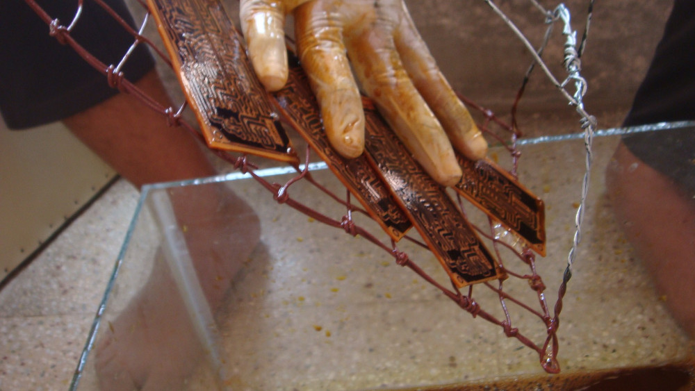
Now that the solution is ready, we can submerge the PCBs into the etchant. For this I made a suspension tray to house the PCBs. Here is a step by step guide on How to Make a Tray to suspend PCBs into the Etchant to make your own tray.

Another important detail is that, the PCBs should not be allowed to settle inside the etchant. This means that you have to keep agitating them. This is when the tray comes in handy.

Keep moving the tray up and down so that the solution is not allowed to settle down. First I put all the 7 boards into the tray and started the etching process but soon realized that it was too crowded and the boards got one over the other. Then I removed 3 of them and continued the process.
Depending on the amount of copper you have to dissolve and the strength of the solution, it might take up to 15 minutes so be patient and keep agitating.
Remove the boards in time!
And as usual, don’t overdo it! The marker pen you used to correct the tracks will not stay on for a long time. Typically the marker will start dissolving only after all the unwanted copper is dissolved.
If you don’t remove the boards once all the excess copper is dissolved the etchant will take the liberty to eat some more copper.
As soon as you remove them from the solution, drop them into a basin with cold water. This will remove the remains of copper and the etchant. After this step you can touch the board.

This is how the PCB looks after the etching process. If you observe carefully you will see that the marker has already started to give away (from the fading color in the copper pour). This is actually the right time to remove the board from the solution.

Remove the toner from the board
Once the etching process is finished, the toner is no longer needed and has to be removed. This can be done in the same way the oxidation was removed. It’s really easy to remove using some detergent and scrubbing the board.

Correct the mistakes you made while cutting
You should have noticed that the boards are irregularly cut and are not of equal size. This is because I made a rough cut and it is nowhere close to being perfect. So to correct those mistakes, take a low grade file and start filing the edges to the correct dimension.
Tip: While making the rough cut, come as close as possible to the exterior line but do not touch it. If the error is positive, we can always file it and correct it - converse is never possible.

Final Result
Here is an image of all the PCBs I made. The whole endeavor took me around 3 to 4 hours. With practice and no time loss in documentation the time taken to make these PCBs should have taken much lesser time.

Now that the PCBs are done, all we have to do is drill the holes and assemble the components. Hopefully from now on I will use one of these programmers/debuggers for posts dealing with PIC Microcontrollers.
I also plan to make some enclosure for this circuit and try to sell some of them to my friends. I will follow up this post soon with another post for the enclosure design.


