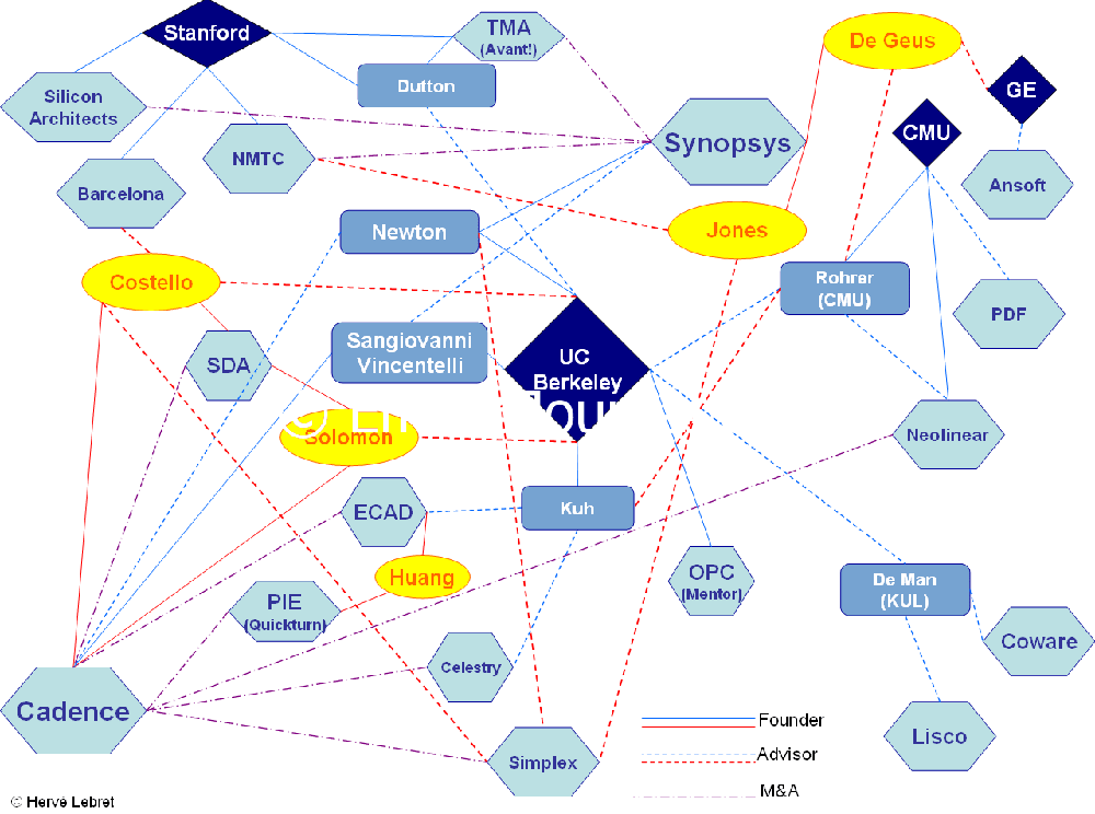
Electronic Design Automation (EDA) is a relatively young five-billion$ industry with a very colorful upbringing, I’m very grateful for, and is an honor to write about it.
EDA involves a diverse set of software algorithms and applications that are required for the design of complex next generation semiconductor and electronics products. The increase in VLSI design complexity poses a significant challenge to EDA; application performance is not scaling effectively, since microprocessor performance gains have been hampered due to increases in power and manufacturability issues, which accompany scaling.
Digital systems are typically validated by distributing logic simulation tasks among huge computer farms for weeks at a time. Yet, the performance of simulation often falls behind, leading to incomplete verification and missed functional bugs. It is indeed no surprise that the semiconductor industry is always seeking for faster simulation solutions.Today EDA employs an estimated more than 30,000 people!.
The current Wikipedia definition of EDA is,
the category of software tools for designing and producing electronic systems ranging from printed circuit boards (PCBs) to integrated circuits. This is sometimes referred to as ECAD (electronic computer-aided design) or just CAD.
The three aspects of EDA are:
- EDA consists of a collection of methodologies, algorithms and tools, which assist and automate the design, verification, and testing of electronic systems.
- It embodies a general methodology that seeks to successively refine a high-level description to low-level detailed physical implementation for designs ranging from integrated circuits (including system-on-chips), to printed circuit boards (PCBs) and electronic systems.
- It involves modeling, synthesis, and verification at every level of abstraction.
History and Evolution:
Before EDA, integrated circuits were designed by hand. Automation first came with geometric software to generate the tapes for the Gerber photoplotter, but even those copied digital recordings of mechanically-drawn components. The process was fundamentally graphic with the translation from electronics to graphics done manually.
By the mid-70s, developers started to automate design with many tools including place and route (P&R).
The next era began about the time of the publication of “Introduction to VLSI Systems” by Carver Mead and Lynn Conway in 1980. This ground breaking text advocated chip design with programming languages that compiled to silicon. The immediate result was a considerable increase in the complexity of the chips that could be designed, with improved access to design verification tools that used logic simulation.
1981 marks the beginning of EDA as an industry. For many years, the larger semiconductor companies developed EDA software internally. In 1981, executives and engineers spun out of these companies to concentrate on EDA as a business. Daisy Systems, Mentor Graphics, and Valid Logic Systems were all founded around this time, and collectively referred to as DMV. Within a few years there were many companies specializing in EDA, each with a slightly different emphasis.
EDA really came into its own with the advent of the ASIC business pioneered by companies like VLSI Technology and LSI Logic. Using excess Japanese manufacturing capacity and building their own fabs locally, they produced Application Specific Integrated Circuits (ASICs) and offered ASIC services for emerging fabless semiconductor companies. A few years later TSMC introduced the fabless semiconductor business model promoting manufacturing efficiencies and commercially available EDA software.
In 1989 the EDA Consortium (EDAC) was founded “To promote the health of the EDA industry, and to increase awareness of the crucial role EDA plays in today’s global economy.” Currently EDAC represents approximately 100 companies around the world.
The success of the EDA field is inspiring for many reasons:
- It has successfully managed the exponential increase in design complexity from the first microprocessor (Intel 4004) with 2,250 transistors to the latest multi-core processor with over a billion transistors.
- It is one of the first fields in computer science and engineering (CS&E) that has applied the concepts and techniques of computational modeling, computational thinking, and computational discovery to an application domain (electronic circuit design) and achieved remarkable success. It has completely transformed the way that electronic engineers design and manufacture integrated circuits. Every circuit being designed today starts with a computational model (specified in an executable programming language) at a high level of abstraction. It then goes through a sequence of synthesis and optimization transformations, followed by rigorous digital simulation and prototyping, as well as formal and semi-formal verification, before it is finally manufactured via advanced lithographical and chemical processes.
- The EDA field is one of the earliest to engage in inter-disciplinary collaboration, where the computer scientists and engineers in EDA successfully collaborated with the electrical engineers to derive various levels of circuit models; with physicists and chemists to derive manufacturing models; with theoretical computer scientists to conduct various kinds of complexity analysis; with applied mathematics and optimization experts to improvise highly scalable simulation and synthesis algorithms; and with application domain specialists to develop intellectual property (IP) libraries, etc.
Today Synopsys, Mentor, and Cadence are the dominant players in the game.
This post is a compilation of information that can be found in various parts of the Internet.


