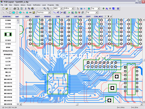
If you haven’t locked yourself in a cave for a couple of years, you would have easily come across this question several times when you went through electronics forums and the discussions in Facebook pages. This is one question that has been directed at me for a very long time by my friends the “best EDA tool”. The answer to the question is quite primitive.
There is no such thing as the best EDA tool. All tools are good as long as there is enough support. Circuit design is an art, like every other art it depends on the designer and not on the design tool used. Industrial softwares come with a heavy $ tag because they have a very good auto routing algorithm. Now, I strongly believe that, no routing algorithm can see through, what even the dumbest of a human brain can, I’m sure the majority of people will believe me in this (Programmers - I am all ears tell me I am wrong :-P) Back to the issue at hand, I prefer doing all the routing manually with all my god-given insight. Besides I want to have my board layout in a single side with minimum jumpers to have a clean etch at home. The details of making a homemade PCB (single sided) will be found here. If manual routing is the case then Altium Designer is no better than KiCad.
There are quite a long list of software packages that are available in the market for you to choose from. If you asked my suggestion, I would recommend KiCad. It’s completely open sourced and under the GNU license and is nowhere close to dying in the foreseeable future. But it has its downsides, it is relatively new and has less support when compared to OrCAD or Eagle and its not very user friendly, again we are engineers we don’t expect friendliness from computers.
The ball is in your court and now it is up to you to decide which software suits your need properly but having the need to learn at least one of these tools have invariably become a must in today’s trend, if you don’t want to be wiped out from the electronics industry.


