Did you know that experienced engineers spend up to an hour on every major component that they are going to be using for upcoming projects? Project as in, real commercial work involving a lot of money and man hour.. not just some hobby project.
When a component is being purchased with a commercial venture in mind, lot of thinking has to be done in various aspects such as the cost, the suitability of the device, the life expectancy, and sustainability of the component in the market long enough for you to make a profit and so on.
But for a hobbyist, life can be much simpler than that but that still doesn’t mean you don’t have to think at all. You do have the advantage of buying a component and start experimenting with it on the run but even then a significant amount of time has to be spent on the datasheet to do anything tangible.
Reading the datasheet and understanding the interface and working of a module from it, is quite possible. All it takes is a little know-how, time and persistence. It might take longer than your conventional way (googling for sample code and circuit diagrams) in the beginning but over time you should be able to do it as fast as or even faster than the conventional way.
Most of the time you will not need everything that is listed on the datasheet. I doubt if there is any application that will demand the use of all the data provided in it. But you will most likely need some basic stuff that are common in all the datasheets.
In this post I discuss some of the key aspects that are common to all the datasheets that you should look out for, when choosing or working with a component.
Overview of the Device
The manufacturer is trying to sell you his product. So almost all the key features of the his product that helps his customers (people like you) find the device easily. Most of the time, the overview is a list of all the features of the device and how its is suitable for the range of applications it was designed for.
So the first thing that you should look for in the datasheet is the overview or summary of the device. This should take up the first or first two pages the datasheet even before the table of contents. Almost all the time, you should be able to tell if this device will suit your need from just seeing these set of points.
Pin Diagram
The next thing to look for is the PIN diagram of the component. There may be a lot of different packages for the same device. Check out the pin diagram for your package. This is especially needed if you are looking for a compatible replacement for a component.
The replacement device must be pin and pad compatible but at least the power and oscillator lines should coincide in the case of an MCU. The others can always be changed in the software. If you plan to use one device for all your development, then I suggest you take a print out of the block diagram and stick it on to the wall near your soldering iron. Trust me, you will be thankful one day!
Application Circuits
A lot of times, I have seen people asking for a “detailed circuit diagram” to be sent to their e-mail because they have to do a project for a college assignment or an event. If you visit some of the How-To section of this blog you will find such statements in the comments section. Honestly, they are the intended audience for this post. When you have access to the datasheet, why would you ask for a circuit diagram? The only possible response is, you don’t know how to use the datasheet effectively.
In almost every datasheet, there is a section that deals with the application of the device. It might just be a description or it might have a detailed circuit with explanation. It must be made a practice to see this regardless of whether you are going to be making the hardware yourself or buying it prebuilt. This knowledge will help when things get a little messy and you have to debug the circuit.
Absolute Maximum Ratings
The absolute maximum ratings are really important as they give you an idea on when your device will be bricked/fried! The manufacturers go to great extents in describing the behavior of the chip at various operational parameters such as voltage, current, temperature and pressure. Most of the time, you don’t have to read everything that is listed. Look for a table like the one below.
It says almost everything that you need to know about the power requirements of the device. You will always have to read the voltage ratings and sometimes the current rating if the device requires more current. (Your SD card, for example, draws a considerable amount of current for its size :P)
Errata Document
You might actually be doing exactly as the datasheet says but the end result may not be as expected. Well it is most likely that you are making the mistake somewhere but one should not rule out the possibility that the documented might be wrong.
Sometimes there are mistakes that the manufacturer made while writing the datasheet that come to light only after the datasheet reaches the user. Sometimes a device may not behave as expected during manufacture. All such mistakes are listed in the errata sheet of the device.
The existence of an errata document for a datasheet can be little hard to come by, but with Google you should be able to find it. It is the responsibility of the user to check the existence of such a sheet and make necessary alteration in the hardware/software.
Timing Diagram
The timing diagrams are mostly used for illustrating protocols. The image below is a timing diagram for the I2C protocol that can be found on the Philips’s specification of the protocol. They help us visualize the state of the pin with the timer interval. It comes in handy when you sit down and start writing low level drivers for hardware protocol.
Besides helping you to write your own libraries for the protocols, it also helps you in understanding the interface better and hence help debug, if something was to go wrong. There you go! Yet another aspect to look out for.
List of associated Registers and their POR values
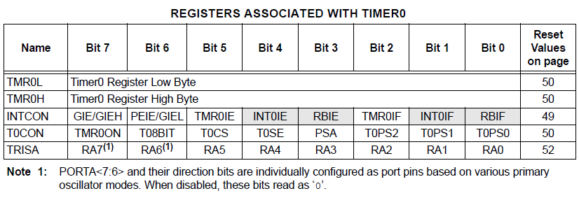
The one thing I find really helpful in PIC microcontroller’s datasheet is, the list of associated registers. If you are using a peripheral for the fist time you will, most probably, read through the entire documentation. But if you are just looking for the names of the registers that are to be modified for the working for the peripheral or checking if you have done everything that is needed for the interface the list of associated registers come in handy. These days I almost always scroll down to this table for all the peripherals.
This table can be found at the end of all the modules in the PIC datasheet. Sometimes not all bits of a register are associated with that particular peripheral. In such cases those bits are grayed out in the table. In the above table, the INTCON register contains the external interrupt and port B interrupt related bits, which are not used for the timer 0 module, hence they are grayed out. It also has the POR (Power On Reset) values of those registers which is nothing but the value that the register will be initialized with upon a reset.
Block Diagrams
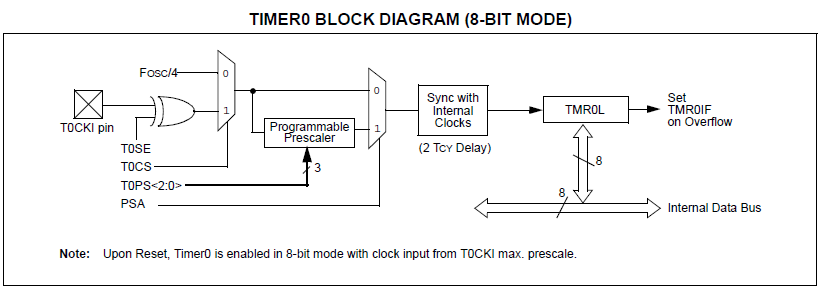
Using the block diagram to understand the behaviour of a module is the most effective way. There are two block diagrams for the Timer 0 module. One, for the 8 bit mode and the other for the 16 bit mode.
The symbols used in the block diagram are simple and understandable. Here is a table to explain the symbols in the block diagram.
**Port Pin: **In most of the block diagrams you will come across a box with a cross in it. This is symbol is used to indicate that a hardware pin is being used as an input/output for the subsequent blocks. In this case it is the external clock input pin.
**Gates: **Logic gate is one that will be there in almost all the datasheets. The symbols for gates are really simple so I’ll not post all of them here. You need to have a working knowledge on gates, flip-flops and their truth table. This is the conventional EX-OR gate. The output is 1 if the inputs are different. If the inputs are same then the output is 0.
**Data Bus: **Sometimes a group of lines starting and ending at the same point have to be represented. Drawing individual lines for all them is a pure waste of time and the diagram looks crappy. That is when this symbol is used to contain all the lines within it. The cut and number next to the arrow indicates the number of lines that it has within it.
**Selection Block: **In most of the embedded modules, you will have to set one bit to have some feature and clear it to have another. This block is used to represent this feature. The green lines are the inputs and the red line is the output. The brown line is a selection bit and can be either 0 or 1. If it is 0 then the input next to the 0 will be connected to the output. Similarly the second input is connected if the selection bit is 1. This is the working of a 2:1 multiplexer. The more the number of input lines the more number of selection lines you will need to multiplex them into one output. To understand this better, you will have to read about multiplexers, demultiplexers, decoders and encoders.
With this basic understanding of the symbols, you should not have any difficulties in understanding the entire working by just seeing the block diagram.
Let’s take a test!
Okay, lets take a short test now! Quite often the block diagram conveys most of the details needed for the interface of that peripheral. Here is the block diagram for the 8 bit mode of operation of the Timer 0 module of PIC microcontroller. Let’s see how much it can tell us about its interface.
Reading from left to right,
The TOSE and the T0CKI pin are given to the ex-or gate.A TOSE (Timer 0 Source Edge select) bit is used to choose if the timer should increment in the high to low transition or in the low to high transition. Basically this gate performs an inverting operation on the external clock if the T0SE bit is set and does nothing if the bit is not set.
The output of the EX-OR gate and the Fosc/4 (system clock) are given to the selection block with T0CS as the selector. The T0CS (Timer 0 Clock Select) bit is used to select the clock for the Timer 0 module. If this bit is set, external clock is used and if it is left cleared, the system clock is used to derive the clock source for the module.
The Programmable Prescaler block. It takes in a 3 bit input (which can be see from the arrow with a 3 cut across it) to determine the prescaler value for the Timer. Read more on prescaler and postscaler. The second selection block as you should have guessed, is used to enable or disable the prescaler. The selector, PSA (Prescaler Assignment) bit if set will enable prescaler and if cleared will disable it.
The internal 8 bit bus (represented by the double headed arrow mark with a cross on it) is used to load the TMR0L register. Now that I have done this one, open a datasheet see if you are able to tell the story from the block diagram.


