The LCD module interface with a microcontroller is simple and it is a primitive means of adding a visual appeal to your embedded application. There are two basic types of LCD modules in the market they are, Character LCD and Graphics LCD. Character LCDs are the some of the cheapest means LCD displays available today.
This post is first of a series of four posts that walks through entire process of interfacing an LCD module with a (any) microcontroller with all the basic concepts dealt in detail. Subscribe to our posts and get free updates on these follow-up posts.
- LCD Module Basic Theory (LCD Controllers, CG&DD RAM, PIN description,Timing Diagram, Commands)
- Programming LCDs in 8 bit mode (programming pic18f4520 in C with C18 compiler under 8 bit mode)
- Programming LCDs in 4 bit mode. (programming pic18f4520 in C with C18 compiler under 4 bit mode)
- Creating Custom Characters (bit map symbols and arrows that are not usually present in the ASCII table)
This post will cover the basic theory that you should have a clear understanding of, before getting started with the programming. Some of the sections below are not really essential for the interface but it is a good practice to have a thorough knowledge about what you are indulging in. Whereas some listed below are absolutely mandatory to understand how the LCD module works and to predict how it will behave for a given situation.
You are free to choose which to read and which to skim (that is if you know what you are doing).
LCD Controllers:
The LCD module has display controller that are used to receive the data from the controller and uses it to display the data in a legible format. These controllers have an embedded font set that can be addressed by sending the corresponding ASCII value of the the character to be printed.
Most LCD modules have a HD44780 or compatible controller which is specially designed to build LCDs with one or two lines with a maximum of 40 character positions each. They are ASIC (Application Specific Integrated Circuit). A single HD44780 is able to display two lines of 8 characters each.
If we want more, the HD44780 has to be expanded with one or more expansion chips, like the HD44100 (2 x 8 characters expansion) or the HD66100 (2 x 16 characters expansion). Seen from the HD44780, the first line starts with 00h; the second line with 40h.
16 x 2 LCD Modules:
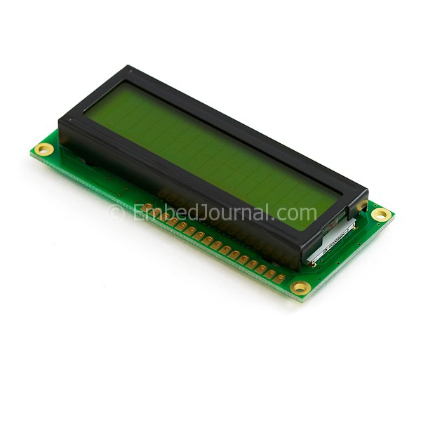
This the most common configuration of LCD that most people prefer mostly due to reduced cost and small footprint. In a 16 x 2 line display LCD module, each the two lines have 40 character positions of which only 16 can be displayed at a time. The remaining positions are invisible and cannot be seen. To display the remaining 24 characters, the LCD has an option to move the window of characters displayed to the right or left so that; it appears as though the characters are scrolling. Here is a table of the DD RAM addresses that are within the visible data region. Note that in this module, DD RAM locations 10 to 27 on the first line and 51 to 67 are not covered by the displayable window of 16A character per line.
| Line/Col | 0 | 1 | 2 | 3 | 4 | 5 | 6 | 7 | 8 | 9 | 10 | 11 | 12 | 13 | 14 | 15 |
|---|---|---|---|---|---|---|---|---|---|---|---|---|---|---|---|---|
| One | 00 | 01 | 02 | 03 | 04 | 05 | 06 | 07 | 08 | 09 | 0A | 0B | 0C | 0D | 0E | 0F |
| Two | 40 | 41 | 42 | 43 | 44 | 45 | 46 | 47 | 48 | 49 | 4A | 4B | 4C | 4D | 4E | 4F |
20 x 4 LCD Module:
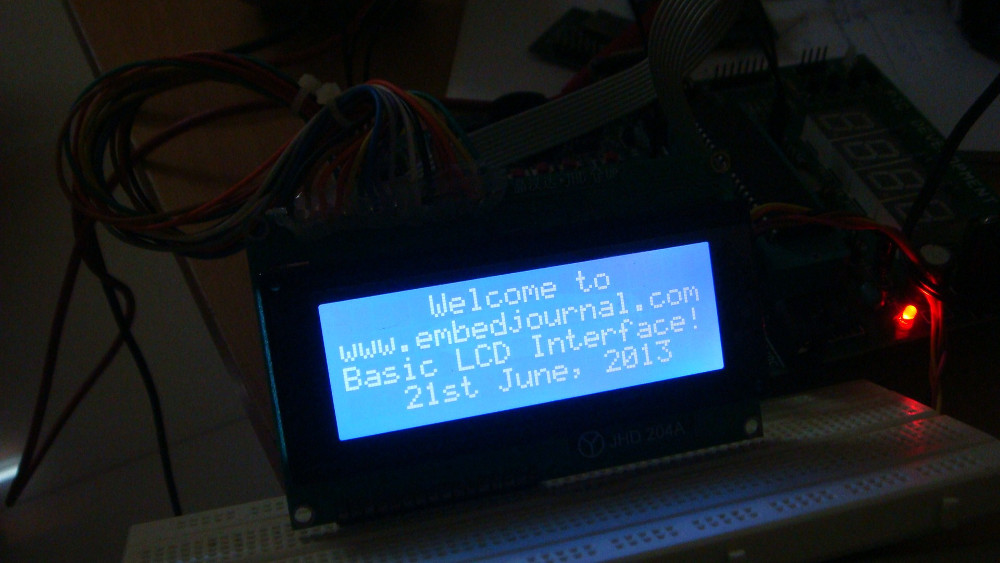
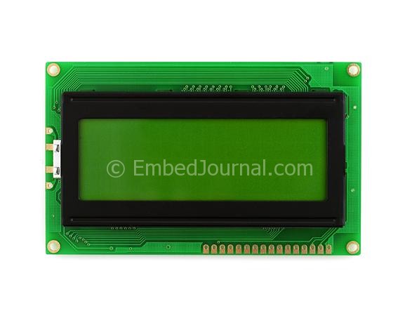
The 20 x 4 display module is a slight variant of the 16 x 2 Module such that, a single 40 character (of which 16 are displayable) line is split up into 2 halves of 20 displayable characters each to make 4 lines. Here the first line displays the first 20 DD RAM locations (00 - 13) and the third line displays the remaining 20 DD RAM locations (14 - 53) of the first line in the case of 16 x 2 LCD Module and the second line displays the first 20 DD RAM locations (40 - 53) and the fourth line displays the remaining 20 DD RAM locations (54 - 67) of the second line in the case of 16 x 2 LCD Module. This is the module that I am using in this post. It has the disadvantage of not being able to scroll but looks better with 4 displayable lines.Here is a table of the DD RAM addresses that are within the visible region.
| # | 00 | 01 | 02 | 03 | 04 | 05 | 06 | 07 | 08 | 09 | 0A | 0B | 0C | 0D | 0E | 0F | 10 | 11 | 12 | 13 |
|---|---|---|---|---|---|---|---|---|---|---|---|---|---|---|---|---|---|---|---|---|
| 1 | 00 | 01 | 02 | 03 | 04 | 05 | 06 | 07 | 08 | 09 | 0A | 0B | 0C | 0D | 0E | 0F | 10 | 11 | 12 | 13 |
| 2 | 40 | 41 | 42 | 43 | 44 | 45 | 46 | 47 | 48 | 49 | 4A | 4B | 4C | 4D | 4E | 4F | 50 | 51 | 52 | 53 |
| 3 | 14 | 15 | 16 | 17 | 18 | 19 | 1A | 1B | 1C | 1D | 1E | 1F | 20 | 21 | 22 | 23 | 24 | 25 | 26 | 27 |
| 4 | 54 | 55 | 56 | 57 | 58 | 59 | 5A | 5B | 5C | 5D | 5E | 5F | 60 | 61 | 62 | 63 | 64 | 65 | 66 | 67 |
PIN Description:
| Pin Number | Name | Description |
|---|---|---|
| 1 | GND (0v) | Ground Potential |
| 2 | VCC (5v) | Positive Voltage |
| 3 | Contrast | Contrast adjustment; 0v: Max contrast; 5v: Min contrast |
| 4 | RS | Register Select; 0: Instruction Register 1: Data Register |
| 5 | RW | Read Write Select pin 0: Write mode; 1: Read mode; |
| 6 | EN | A Enable Pin To enable the LCD Module |
| 7 | DB0 | LCD Data Bus line. They are responsible for the parallel data transfer. DB7 is used to check the busy Flag.In 4 bit mode, DB0 to DB3 are not used and are left open. |
| 8 | DB1 | |
| 9 | DB2 | |
| 10 | DB3 | |
| 11 | DB4 | |
| 13 | DB5 | |
| 14 | DB6 | |
| 15 | DB7 | |
| 16 | A LED+ (A) | A Back Light Source LED Anode |
| 17 | LCD- (K) | Back Light Source LED Cathode |
Registers:
There are two registers in an LCD, they are Instruction register and the Data register. The register select (RS) pin is used to select either of the two the registers. When held low, the Instruction register is selected and similarly, when it is high, the data register is selected. A write to the data register will write to the Display Data RAM (DD RAM) in the address last pointed by the address pointer. The address pointer is automatically incremented after each write operation.
In the 20 x 4 LCD Module, all the locations of the DD Ram are mapped on to a character position in the display. Hence a write to the data register with proper ASCII code will produce proper displayable character in the screen. You can find a good ASCII table here. Some of the values in the ASCII table are not printable and hence are not mapped on to any character. A write to the DD Ram with one such data will display some glyph that you cannot recognize.
The LCD datasheet comes with a lot of electrical and Mechanical specifications. Though they are not redundant, for now we will consider only the command sheet and the timing diagram without which it is impossible to interface the module.
Command Sheet:
The command sheet is a table which contains the various commands that can be issued to the LCD module so that it behaves as intended. I have not attached an image of the command sheet as I could not find any of a good readable resolution. So I created a HTML version of the command sheet that you could use at any resolution dYtm, You can find the Command Sheet here (or I should call it command page). The cells that are filled with absolute values have to be used as such and the ones that are having letters are variables and take either 0 or 1 based on the task it has to perform.
For example, the Display ON/OFF Control command has the following fields,
| RS | R/W | D7 | D6 | D5 | D4 | D3 | D2 | D1 | D0 |
|---|---|---|---|---|---|---|---|---|---|
| 0 | 0 | 0 | 0 | 0 | 0 | 1 | D | C | B |
Here, D4 to D7 are 0, D3 is 1 and RS and R/W are held low. These are all constant values and hence have to be used as such. But the, bits D0 to D2 are all variables. Depending on the values return at positions B, C and D the following action are performed by the LCD controller,
D set to 0/1 Turns the display ON/OFF
C set to 0/1 Turns the Cursor ON/OFF
B set to 0/1 Character at the cursor is static/blinking
According to this description, the value has to be written to the command register. That is if you want, display ON, cursor ON and the character at the cursor to be static, you have to write, 0x0E while holding the RS and RW lines Low.
Timing Diagrams:
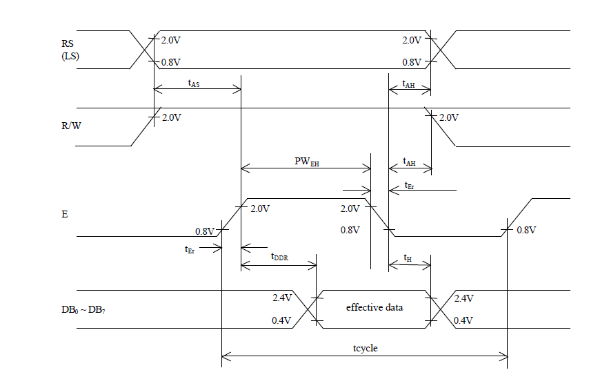
There are two basic timing diagrams, one for the read operation and another for the write operation. Both of them are very important and has to be adhered to. Reading and understand timing diagrams is an important skill that has to be mastered.
Read Operation:
Write Operation:
Yet another timing diagram!
Lastly, here is another timing diagram that you will be hard pushed find else where. Incidentally, it is not only the software that need to be initialized, but hardware too. You could use hardware timing to initialize the module. Here is its description.
Microcontroller Pin Requirements:
As you know these LCDs have a built in font set and can be used by indexing the ASCII value of the corresponding character. It capable of operating on 8 data lines (D0 to D7) or on 4 data lines (D4 to D7). The upcoming posts will discuss the 8 bit and 4 bit mode of LCD interface. Other than the data lines the LCD needs 3 command lines - RS, R/W and EN. Therefore in total, an LCD interface will need 11 (8+3) or 7 (4+3) pins of the microcontroller.
It is possible to further reduce the total number of port pins required from 7 (4+3) to 6 (4+2) by shorting the R/W pin to ground. If the R/W pin is connected to the ground, the LCD can be used to write data only. Reading from it is not possible. So we are not able to read the busy flag from the module. To live with this disability, we are forced to provide ample amount of delay loops (and hence compromise on the speed of execution) so that the LCD is seldom busy doing thing when new data is given.
Update: Part 2 of this post in now available here.


